


Top casino winners from New Zealand - list of winners, success stories
Top casino winners from new zealand. New Zealand is a country that is known for its rich cultural heritage, picturesque landscapes and the hospitality …
Read Article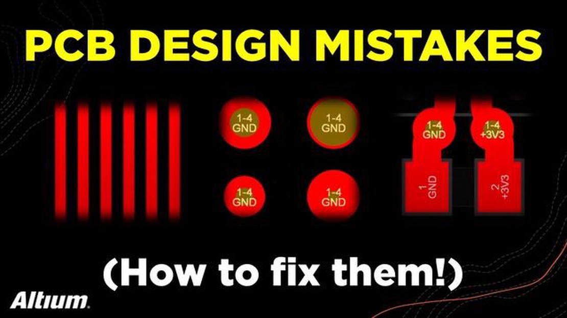
Making printed circuit boards is an important step in the process of creating electronic devices. They allow you to connect all the components together and ensure that the device works properly. For novice engineers, making PCBs can seem like a daunting task. However, with some tips and guidelines, you will be able to successfully handle the process.
The first step in PCB fabrication is to create a schematic diagram of your device. Circuit design programs are now available to almost everyone. You can use one of these programs to create a schematic of your device. Remember that a clear and understandable schematic is the foundation of successful PCB fabrication.
After creating the schematic, you need to develop a PCB layout. The PCB layout defines the location of each component on the board and the routing steps of the traces (conductors) connecting the components. You can use a PCB design program to create the layout. It is important to consider the size and shape of your device when designing the PCB layout.
Hint: When designing a PCB layout, it is recommended that you use what is known as the “angel rule” - trace the conductors so that they form a 45 degree angle. This will reduce the chances of crossing conductors and increase the reliability of your PCB.
Making PCBs is one of the important steps in creating electronic devices. If you are a beginner in this field, you may find some useful tips helpful.
Before you start designing a printed circuit board, you need to choose the right software. There are many programs available such as Altium Designer, Eagle, KiCad and others. Choose a program that suits your needs and that you can learn. 2. **Learn how to work with components.
Determine what components will be used on your PCB. Study their parameters and assembly rules. This will help you avoid assembly errors and allow you to create a more reliable device. 3. **Place the components on the printed circuit board.
It is very important to properly place components on the printed circuit board. Placement can affect the routing and EMC of the device. Pay attention to component placement rules and manufacturers’ recommendations. 4. **Routing of traces.
Proper routing of traces on the PCB is very important to ensure quality operation of your device. Pay attention to the boundary conditions and recommendations for each trace. 5. Check your design.
Be sure to verify your design before sending your PCB to production. Use available tools to automatically verify integrity and EMC. By checking your design, you will be able to correct errors before the board is manufactured. 6. Selecting a manufacturer.
Choosing a reliable PCB manufacturer is an important step. Study reviews and testimonials from other designers. Pay attention to technological capabilities and lead times.
By following these tips, you will be able to improve the quality of your PCBs and create more reliable devices. Good luck with your projects!
Making printed circuit boards can be a complex process, especially for beginners. This expert guide covers basic tips and tricks to help you get the job done.
Before you start creating a printed circuit board, you need to make thorough preparations. This includes choosing the right PCB design software, learning the basic design principles and rules, and familiarizing yourself with basic technologies and materials.
The choice of material for PCB manufacturing is critical to the quality and reliability of the final product. FR-4 is recommended because it provides good electrical isolation, dimensional stability, and mechanical strength.
Before you send your board to production, a careful design should be done. Make sure that all components are properly located and connected to each other, check that there are no overlaps or short circuits.
Proper board layout is critical to the efficient operation of electronic components. Consider minimizing parasitic elements, placing high-power elements close to the power supply and signal traces close to each other.
Before you send your board to production, it is recommended to check its performance. This can be done using special software that allows you to simulate the operation of the board and detect possible errors or problems.
Read Also: 7 Best Flip Phones in 2023 | Top Picks and Reviews
Components should be installed according to the manufacturer’s instructions. It is important to orient the components correctly, solder them properly, and verify that there are no shorts or bad contacts.
Don’t forget to make marks and inscriptions on the board to make it easier to orient components and traces. This will save you time when servicing and repairing the board later.
Once you receive the PCB from production, it is recommended that you thoroughly inspect it before installing it in the final device. Check for shorts, proper installation of components and connections, and the operation of all functions.
By following these tips, you will be able to produce a high-quality PCB that will ensure that your electronic device functions reliably and efficiently.
Read Also: How to Enable Music Share on Samsung Galaxy Tab S6
When creating printed circuit boards, one of the most important steps is choosing the right materials. Choosing the right materials can make a big difference in the quality and reliability of the board.
Here are some tips to help you choose the right materials:
Remember that selecting PCB materials is an important step in the process of creating a reliable and efficient board. Analyze the project requirements and consider the above tips to make the right choice.
Creating a PCB schematic is an important step in the electronic manufacturing process. Proper circuit design can improve the functionality and efficiency of the PCB, as well as reduce the possibility of errors and distortions in the device.
It is recommended to use specialized programs such as Eagle, Altium Designer, KiCad, etc. for PCB schematic design. These programs provide a user-friendly and intuitive interface for creating and modifying the schematic.
Here are some tips to help you develop a proper PCB schematic:
Creating a proper PCB layout is an important step towards the successful development of an electronic device. By following the above tips, you will be able to improve your design process and get a quality PCB for your project.
The PCB manufacturing process is an important step in the creation of electronic devices. It includes several features that need to be considered when designing PCBs.
In addition, various problems can occur during the PCB manufacturing process such as improper conductor connections, short circuits, poor conductivity, etc. It is important to have the experience and knowledge to prevent and solve these problems.
Thus, the PCB manufacturing process is a complex and important part of a project that requires attention to detail, experience and technical knowledge. But with the right approach, it can produce quality and reliable PCBs for various electronic devices.
Various materials such as foil, glass-textolite, ink and photo-resistant film are commonly used to make printed circuit boards. The foil is used as conductors, the fiberglass is used as the base for the board, the ink is used to create the conductors, and the photocurable film is used to show the layout of the board.
There are several ways to create a PCB layout. One of the most common is to use PCB design software. The program can be downloaded from the web and is usually free. You need to design the PCB layout on the computer, then send the design to manufacturing. Another method is to manually create a PCB layout using foil, scissors, and duct tape.
The time it takes to make a PCB depends on the method you choose and your level of experience. If you use design software, the process can take a few days or weeks depending on the complexity of the design and the speed of order processing. In the case of manually creating a layout, the time can vary, but it usually takes about a day.
If the PCB does not work after manufacturing, the first thing to do is to check all connections and conductors for errors or breaks. It is also worth checking the correct connection of components to the board and their position. If the problem cannot be solved, you can contact specialists or electronic engineering communities for help and advice.
There are many companies that manufacture printed circuit boards. You can find them on the Internet by searching for “PCB fabrication” or “order a PCB”. Also in some cities you can find workshops or electronics centers where you can order the manufacture of printed circuit boards. It is recommended to pay attention to reviews and ratings of companies to choose a reliable performer.
A printed circuit board is a special plastic board on which electronic components are located. It is used to make electrical connections between the components and ensure proper operation of the electronic device.
Top casino winners from new zealand. New Zealand is a country that is known for its rich cultural heritage, picturesque landscapes and the hospitality …
Read Article
How to Fix WWE 2K23 Unable to Communicate with the Server Are you experiencing the “Unable to Communicate with the Server” issue while trying to play …
Read Article
How To Use Wireless Charger Wireless charging has become increasingly popular in recent years, as it offers a convenient and clutter-free way to …
Read Article
Do favorites usually win in Super Bowl futures betting? . The Super Bowl is one of the biggest sporting events of the year, bet on by millions of …
Read Article
What to do if Galaxy J3 can’t receive texts from one contact only If you own a Samsung Galaxy J3 and are experiencing difficulties receiving text …
Read Article
Hearts of Iron IV Won’t Download? Here’s how to fix it Hearts of Iron IV is a popular strategy game that allows players to take control of a nation …
Read Article


